
The blog is dedicated to provide an overview of the C band RF Transceiver’s design, specifications, and functionality. It emphasizes the importance of the transceiver in enabling wireless communication between the ground and satellites, especially in challenging terrains.
C band RF transceiver are crucial components in wireless systems, particularly in VSAT systems or Earth stations. The transceiver facilitates wireless connectivity between the ground and satellites.
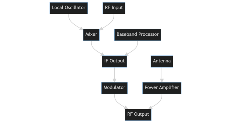
The key points of design and development of a C band RF transceiver are summarized below in Figure 1.
C band RF Transceiver Overview:
- Purpose: Converts modulated IF into RF and vice versa.
- Components: RF Up converter, RF down converter, 10MHz OCXO, RF synthesizer, Local oscillator, RF power divider, IF power divider, M & C card, power supply.
- Usage: In VSAT systems for voice and data call connections in various terrains.
Specifications:
- Transmitter:
- Input frequency: 52 to 88 MHz
- Output frequency: 5925 to 6425 MHz
- Conversion Gain: 20 dB minimum
- Gain flatness: +/- 1 dB over entire band
- 1 dB compression point: better than +3dBm
- Spurious and harmonics level: better than -40 dBc
- Receiver:
- Input frequency: 3.7 to 4.2 GHz
- Output frequency: 52 to 88 MHz
- Conversion Gain: 40 dB minimum
- Noise Figure: better than 14dB
- Image rejection: better than -50dBc
- Spurious and harmonics level: better than -40 dBc
Block Diagram Explanation:
- The RF Transceiver interfaces with a modem on one side and with PA/LNA on the other.
- It has two main parts: Up converter and down converter.
- Up converter: Converts modulated IF IN (70+/-18 MHz) into modulated RF OUT (5925-6425MHz).
- Down converter: Converts modulated RF IN (3700-4200) MHz to IF OUT (70+/-18 MHz).
Design Guide:
- The RF Transceiver is made up of two major modules: RF up converter and down converter.
- The up converter converts a lower frequency to a higher frequency, while the down converter does the opposite.
- The design uses discrete RF components, with a microstrip line etched on a PCB for soldering these components.
- Dual conversion approach is used in the up converter.
- Two RF mixers in both the up and down converters follow the Heterodyne Architecture design.
10MHz OCXO:
- This RF oscillator serves as a reference for both the IFLO and synthesizer in the RF Transceiver.
